
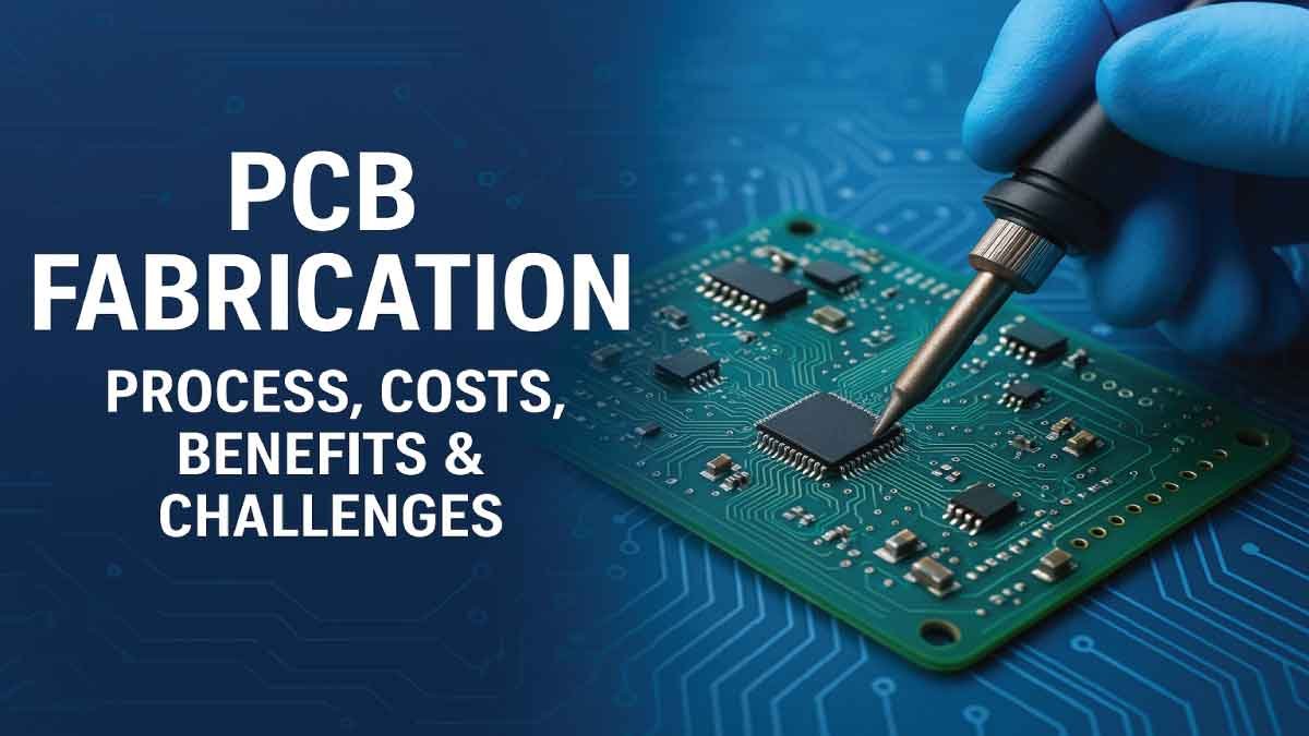
PCB Fabrication is a pivotal process in the world of electronics, ensuring that your circuit designs are transformed into functional, reliable boards used in countless devices. In this blog post, we will break down everything you need to know about PCB fabrication, from the very basics to the intricate details that go into making a high-quality PCB.
So, what exactly is PCB fabrication? At its core, PCB fabrication refers to the creation of a printed circuit board (PCB), which serves as the foundation for electronic components. Understanding PCB fabrication meaning and PCB fabrication definition is crucial to grasping how devices like smartphones, computers, and many other electronics are built.
In addition to the general process, we will also explore what is PCB designing and fabrication and how these two crucial stages work together to bring a design to life. To make sure everything is done correctly, it’s important to understand what files are needed for PCB fabrication, as the right files are essential for precise manufacturing.
We will also dive into the PCB fabrication process challenges and how they can affect the final product. Ever wondered what is PCB fabrication process from start to finish? Don’t worry, we will walk you through a detailed step-by-step guide so you can get a clear understanding of the entire procedure. Additionally, we will provide a detailed overview of the PCB manufacturing process flow chart to visually represent the sequence of steps involved.
Cost is another critical factor in PCB fabrication. We’ll take a look at PCB fabrication cost and discuss the various factors that influence what affects the price during the manufacturing process.
Finally, we will highlight the uses and benefits of PCB fabrication, explaining why it’s an essential process for virtually every electronic device today.
By the end of this blog post, you will have a thorough understanding of PCB fabrication, from its basic concepts to the challenges and factors that affect cost, along with its wide-ranging applications and benefits. Let’s dive in and explore this fascinating topic!
What is PCB Fabrication?
PCB fabrication is the process of manufacturing printed circuit boards, which are essential components in almost all electronic devices. It starts with designing the PCB layout, followed by transferring the design onto a physical board using layers of copper and insulating material. Holes are drilled, copper traces are etched, and components are later mounted on the board. This process ensures that electrical signals flow correctly between parts. PCB fabrication requires high precision and quality control, as even small mistakes can cause a device to malfunction. It’s a critical step in bringing electronic ideas to life.
PCB Fabrication Meaning:
PCB fabrication means the process of building a printed circuit board from a design layout. It includes steps like layering materials, etching copper traces, drilling holes, and preparing the board for electronic components. This process transforms a digital design into a working physical board used in gadgets, computers, cars, and more. Without PCB fabrication, we wouldn’t be able to power most of the modern electronics we rely on every day.
PCB Fabrication Definition:
PCB fabrication is the technical process of creating a printed circuit board (PCB) that allows electronic components to connect and function properly. It involves multiple steps such as layout printing, layering insulating and conductive materials, etching circuits, and drilling holes. The goal is to create a functional board that routes electrical signals as designed. This definition includes both the physical building of the board and the quality checks needed to ensure it works reliably in electronic devices.
What is PCB Designing and Fabrication?
PCB designing and fabrication are two essential stages in creating a printed circuit board used in electronic devices. PCB designing involves creating a digital layout of the circuit using specialized software like Altium, Eagle, or KiCad. This layout defines where components will go, how they connect, and how electrical signals will flow. Once the design is finalized, it’s converted into manufacturing files called Gerber files.
PCB fabrication is the process of turning that digital design into a physical board. This includes layering copper, etching circuit paths, drilling holes, applying a solder mask, and adding a surface finish. Together, designing and fabrication form the complete workflow of producing a reliable PCB for electronic use, from concept to functional hardware.
What Files Are Needed for PCB Fabrication?
Creating a printed circuit board (PCB) involves two major steps—design and fabrication. Once you’ve designed your PCB using software like KiCad, Altium Designer, or Eagle, the next step is fabrication, where the digital design is transformed into a physical board. But to do this, the manufacturer needs specific files that contain all the information required to build the board correctly.
Below is a detailed breakdown of the essential files needed for PCB fabrication.
1. Gerber Files
Gerber files are the most critical set of files required for PCB fabrication. They are standard file formats that describe the different layers of a PCB. Each layer of your board design—such as copper layers, solder masks, and silkscreens—requires its own Gerber file. These files help the manufacturer know where to put copper traces, where solder mask should be applied, and what markings or labels go on the board.
The main Gerber files include:
Top Copper Layer – Shows the electrical connections on the top side.
Bottom Copper Layer – Shows connections on the bottom side.
Solder Mask Layers (Top and Bottom) – Indicate where the solder mask should be applied.
Silkscreen Layers (Top and Bottom) – Contain component labels, reference designators, and logos.
Inner Layers – Used in multilayer boards for power and ground planes or complex routing.
Board Outline (Mechanical Layer) – Defines the exact shape and edge cuts of the board.
2. Drill File (Excellon Format)
The drill file tells the manufacturer where to drill holes for vias, through-hole components, and mounting points. It also specifies hole sizes and whether the holes are plated or non-plated. This file is typically in Excellon format and must be accurate, as drilling errors can affect board functionality.
3. Netlist File (Optional but Helpful)
A netlist is a file that lists all the electrical connections between the components. Although not always required by the fabricator, it can help during electrical testing to ensure that the board has no short circuits or broken connections.
4. Pick and Place File (For Assembly)
If you’re also having your board assembled (with components soldered), then a pick and place file is essential. It contains the exact position, rotation, and side (top or bottom) of each component. This file is used by automated machines to correctly place components on the PCB.
5. Bill of Materials (BOM)
The BOM is a list of all the components used in the PCB design, including part numbers, quantities, and descriptions. While it’s not needed for fabrication alone, it’s required if you’re getting the board assembled.
To successfully fabricate a PCB, you must provide accurate and well-prepared files. At the very least, Gerber files, a drill file, and a board outline are mandatory. For assembly services, a BOM and pick and place file are also necessary. Always double-check your files before sending them to a manufacturer to ensure smooth and error-free PCB production.
PCB Fabrication Process Challenges
PCB fabrication is a complex and precise process, and despite advances in technology, several challenges can arise along the way. These issues can impact the performance, reliability, and cost of the final product. Understanding the common challenges in PCB fabrication helps designers and manufacturers work together more effectively to produce high-quality boards.
1. Design Complexity and Miniaturization
As electronic devices become smaller and more powerful, PCB designs are growing increasingly complex. High-density interconnect (HDI) boards, fine-pitch components, and multiple layers are harder to fabricate. Maintaining precision in such compact designs is a major challenge, especially during etching, drilling, and layer alignment.
2. Tight Tolerances
Modern PCBs often require extremely tight tolerances in trace width, spacing, and drill hole alignment. Even a slight deviation can lead to short circuits, open circuits, or signal integrity issues. Manufacturers need highly calibrated equipment and careful quality control to meet these demands.
3. Material Selection Issues
The choice of base materials (like FR4, polyimide, or Rogers laminates) affects the board’s thermal, electrical, and mechanical properties. Selecting the wrong material can result in warping, delamination, or failure in high-temperature or high-frequency environments. Balancing cost with performance is often a challenge.
4. Drilling and Plating Defects
Drilling tiny, precise holes (vias) and plating them with copper is a sensitive step. Common problems include misalignment, incomplete plating, or rough hole walls. These defects can lead to weak connections between layers, causing intermittent faults or board failure.
5. Solder Mask and Silkscreen Problems
Improper solder mask application can cause solder bridging during component assembly, leading to short circuits. Similarly, poor silkscreen printing can affect readability, making manual assembly or inspection harder. These layers require accurate alignment and clean application.
6. Thermal Management
With high-speed components and power-dense designs, managing heat dissipation is crucial. Boards not designed or fabricated with adequate thermal management features (like thermal vias, copper pours, or heatsinks) may overheat and degrade quickly. Ensuring the board performs reliably under thermal stress is a key challenge.
7. Quality Control and Inspection
Detecting microscopic defects such as hairline cracks, improper etching, or incomplete vias can be difficult without advanced inspection methods like AOI (Automated Optical Inspection), X-ray testing, or flying probe testing. Skipping proper quality control can result in faulty boards reaching the customer.
8. Cost vs. Performance Trade-Offs
Balancing cost, performance, and manufacturability is a constant challenge. High-performance boards often require premium materials, more layers, and tighter tolerances—driving up production costs. Designers and fabricators must collaborate to find a cost-effective yet reliable solution.
PCB fabrication is a finely tuned process with many variables that must be controlled. By understanding the common challenges—ranging from material choices to precision drilling—both designers and manufacturers can take proactive steps to ensure quality and performance. Addressing these issues early leads to better, more reliable electronic products.
What is PCB Fabrication Process? (Step-by-Step Guide)
PCB (Printed Circuit Board) fabrication is the process of creating a physical board that connects and supports electronic components. It transforms a PCB design into a working board using various materials, machinery, and steps. Whether it’s for a simple device or a complex gadget, the process needs to be precise and reliable.
Here’s a step-by-step guide to the PCB fabrication process:
1. Design and Output Files
The process starts with a digital design, usually created using software like Eagle, Altium, or KiCad. The design includes the circuit layout, layer information, drill holes, and component placements. These files are converted into Gerber files, which manufacturers use to understand how the board should look and function.
2. Design Review and DFM Check
Before actual fabrication, the manufacturer checks the Gerber files using a DFM (Design for Manufacturability) analysis. This step ensures the design can be physically built without errors. It helps identify issues like trace width, spacing, hole alignment, or missing layers.
3. Printing the PCB Layout
The PCB layout is printed onto a film or photoresist using a laser plotter. This step creates a precise image of the PCB layers, including where copper will remain and where it will be removed.
4. Creating the Substrate
The base material, usually fiberglass (FR4), is cleaned and prepared. Copper foil is laminated onto it, forming the base for electrical paths. A photoresist layer is applied on top, which will help define the copper traces.
5. Image Transfer and UV Exposure
The photoresist-covered board is aligned with the printed film and exposed to UV light. The UV light hardens the exposed photoresist, creating a mask. The unhardened photoresist is then removed, exposing the copper that needs to be etched away.
6. Etching the Copper
The board is passed through a chemical solution that removes unwanted copper. Only the copper covered by hardened photoresist remains, forming the required circuit paths.
7. Drilling Holes
Next, holes are drilled into the board for mounting components or creating vias (connections between layers). Drilling must be highly accurate, especially for multilayer PCBs.
8. Plating and Copper Deposition
After drilling, the holes are plated with copper to make them conductive. This step allows electrical signals to pass through layers of the board.
9. Solder Mask Application
A solder mask layer is applied to protect the copper traces from oxidation and prevent solder bridges during component soldering. This is typically the green (or other colored) coating you see on PCBs.
10. Silkscreen Printing
Text and symbols like part labels, logos, and identifiers are printed on the board using silkscreen. This helps in component placement during assembly.
11. Surface Finish
A surface finish such as HASL (Hot Air Solder Leveling), ENIG (Electroless Nickel Immersion Gold), or OSP (Organic Solderability Preservatives) is applied to exposed copper areas to enhance solderability and longevity.
12. Final Inspection and Testing
Finally, the PCB is inspected visually and electrically to detect any shorts, open circuits, or design mismatches. Automated optical inspection (AOI) and flying probe tests are commonly used.
PCB fabrication is a detailed, multi-step process that brings electronic designs to life. From digital layout to a working board, each step must be done with precision. This ensures that devices function reliably, whether they’re in your phone, car, or a satellite in space.
See This Video Guide: PCB Fabrication Process:
PCB Fabrication Cost: What Affects the Price?
The cost of PCB fabrication can vary significantly depending on several factors. Whether you’re prototyping a simple 2-layer board or ordering a high-volume run of complex multilayer PCBs, understanding what affects the price can help you make better decisions and manage your budget.
1. Number of Layers
A 2-layer PCB is cheaper to fabricate than a 4-layer or 6-layer one.
More layers mean additional materials, drilling, alignment, and complexity in manufacturing.
2. Board Size and Quantity
Larger boards use more material, increasing the cost.
Ordering in bulk significantly reduces the cost per board due to economies of scale.
3. Material Type
Standard FR4 is inexpensive.
High-frequency or high-temperature materials like Rogers or polyimide are more expensive but necessary for specialized applications.
4. Trace Width, Spacing & Tolerances
The tighter the tolerances and finer the traces, the higher the precision required—leading to increased cost.
High-density designs also require advanced processes.
5. Surface Finish
Basic HASL (Hot Air Solder Leveling) is affordable.
ENIG (Electroless Nickel Immersion Gold) or OSP (Organic Solderability Preservative) finishes improve performance but raise the price.
6. Drill Hole Size and Count
A board with many vias or tiny holes (microvias) requires precision drilling, which adds to the cost.
Laser drilling for HDI boards is especially expensive.
7. Lead Time (Turnaround Time)
Faster delivery (e.g., 24–48 hours) significantly increases cost.
If you can wait longer (7–10 days), you can save money.
8. Special Requirements
Requirements like impedance control, blind/buried vias, flex or rigid-flex boards, or edge plating all add complexity and cost.
Typical Price Range (as of 2025):
Prototype 2-layer PCB (5 pcs, small size): $5–$20 (e.g., from JLCPCB or PCBWay)
4-layer PCB (small batch): $30–$100
Multilayer high-speed PCB (10+ layers): $150 and up per board
The cost of PCB fabrication depends on the design’s complexity, material selection, layer count, and delivery time. For basic prototypes, the price can be very low thanks to global manufacturers offering cheap services. But for advanced boards with specific technical demands, the cost increases significantly. Careful planning during the design phase can help reduce unnecessary costs.
PCB Fabrication Uses
PCB (Printed Circuit Board) fabrication is essential in building nearly every modern electronic device. It involves creating the physical board that connects and supports electronic components. Here are the main uses of PCB fabrication:
1. Consumer Electronics
Used in smartphones, laptops, tablets, TVs, gaming consoles, and wearable devices.
Enables compact, reliable, and mass-producible electronics.
2. Industrial Equipment
PCBs are used in control systems, automation devices, power supplies, and sensors.
Rigid and high-temperature-resistant boards are common in harsh environments.
3. Medical Devices
Found in diagnostic machines (ECG, MRI), implants, and portable monitors.
Requires highly precise and reliable boards, often with strict safety standards.
4. Automotive Electronics
Used in engine controls, GPS systems, sensors, and electric vehicle components.
Requires PCBs that can withstand vibrations, heat, and moisture.
5. Telecommunications
Essential in routers, signal boosters, satellites, and mobile towers.
High-frequency and multilayer PCBs are common for fast signal processing.
6. Aerospace and Defense
Used in radar systems, aircraft controls, drones, and communication devices.
Must be extremely reliable and often built with high-end materials.
7. LED and Lighting Systems
PCBs are used to mount and power LEDs in lighting panels, displays, and signs.
Aluminum-backed PCBs help with heat dissipation.
PCB fabrication plays a vital role in making modern technology possible. From daily gadgets to life-saving medical tools and advanced aerospace systems, PCBs are the foundation of electronic functionality and performance.
Would you like visuals or industry-specific examples for this topic?
PCB Fabrication Benefits
PCB fabrication offers several key advantages that make it essential for modern electronics manufacturing. Here are the major benefits:
1. Compact and Lightweight Design
PCBs allow for compact layouts, where components are neatly organized and connected. This reduces overall device size and weight, which is crucial for smartphones, wearables, and compact gadgets.
2. High Reliability
Fabricated PCBs are durable and long-lasting. They withstand physical stress, heat, and vibrations better than traditional wired circuits, ensuring consistent performance over time.
3. Consistent Quality and Repeatability
Once a PCB is designed, it can be fabricated with high precision in large quantities—ensuring each board is identical. This consistency boosts product quality and reduces defects.
4. Time and Cost Efficiency
Mass production of PCBs reduces manufacturing time and cost. Automated assembly and standardization allow faster turnaround and lower labor expenses compared to manual wiring.
5. Easy Maintenance and Diagnostics
PCBs make it easier to identify and fix faults. Clear silkscreen labels and organized layouts simplify testing, troubleshooting, and component replacement.
6. Supports Complex Designs
Modern PCBs can support multilayer, high-speed, and high-frequency circuits, making them ideal for advanced electronics, including communication and computing devices.
7. Reduced Electronic Noise
With careful design, PCBs help minimize electromagnetic interference (EMI) and crosstalk between components, leading to better signal integrity and overall performance.
8. Environmentally Friendly Options
Many manufacturers offer lead-free and RoHS-compliant fabrication options, reducing the environmental impact and making devices safer for users.
PCB fabrication delivers efficiency, reliability, and scalability—making it a cornerstone of the electronics industry. Whether for consumer tech, automotive systems, or industrial controls, the benefits of PCB fabrication drive innovation and progress.
Conclusion:
In conclusion, PCB fabrication is a complex yet essential process that transforms electronic designs into the functional boards that power our devices. From understanding the PCB fabrication meaning and PCB fabrication definition to grasping the nuances of what is PCB designing and fabrication, it’s clear that this process is both intricate and critical. Knowing what files are needed for PCB fabrication ensures the manufacturing process runs smoothly, while being aware of PCB fabrication process challenges can help prevent errors along the way.
By now, you should have a clear understanding of what is PCB fabrication process, thanks to our detailed step-by-step guide and PCB manufacturing process flow chart. Additionally, we’ve explored the various factors that influence PCB fabrication cost and what specifically affects the price.
Finally, the uses and benefits of PCB fabrication are vast, making it an indispensable part of the electronics industry. Whether you’re designing for consumer electronics, industrial machinery, or cutting-edge technology, understanding the ins and outs of PCB fabrication will help ensure the quality and efficiency of your final product.
With the knowledge you’ve gained from this post, you now have a deeper insight into the world of PCB fabrication, and you’re equipped to approach this process with confidence.
FAQs:
What is the difference between PCB designing and PCB fabrication?
PCB designing is the process of creating the layout of the circuit board, including the components, traces, and connections. PCB fabrication is the process of physically manufacturing the board based on the design, involving steps like etching, drilling, and applying solder masks.
What files are required for PCB fabrication?
For PCB fabrication, designers typically need Gerber files, bill of materials (BOM), and drill files. These files provide all the necessary data to manufacture the PCB, including the layout, component details, and hole drilling specifications.
What are the benefits of PCB fabrication in modern electronics?
PCB fabrication enables the production of durable, compact, and efficient electronic circuits. The process supports high-density designs, increased reliability, cost-efficiency, and versatility, making it essential for industries like telecommunications, automotive, and consumer electronics.
What are the main steps involved in the PCB fabrication process?
The PCB fabrication process involves several critical steps, including PCB designing, file preparation, material selection, etching, drilling, solder mask application, testing, and final inspection. Each step plays a vital role in ensuring the final product is functional and reliable.
How does the PCB fabrication cost vary depending on the project?
PCB fabrication cost depends on factors like design complexity, material choices, size, layer count, and the required quantity. PCB fabrication process challenges such as tight tolerances, advanced features, and quick turnarounds can also influence the final price.